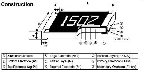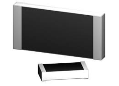
The resistive material is a special paste with a mixture of a binder, a carrier, and the metal oxides to be deposited. The binder is a glassy frit and the carrier exists of organic solvent systems and plasticizers. Modern resistor pastes are based on oxides of ruthenium, iridium and rhenium. This is also referred to as a cermet (Ceramic – Metallic). The resistive layer is printed onto a substrate at 850°C. The substrate is often 95% alumina ceramic. After the firing of the paste on the carrier, the film becomes glasslike, which makes it well protected against moisture. The thickness is in the order of 100 micrometer. This is approximately 1000 times more than thin film. Unlike thin film, this process is additive. This means that the resistive layers are added sequentially to the substrate to create the conducting patterns and resistance values.

The temperature coefficient of thick film resistors typically ranges from 50 ppm to 200 ppm/K. Tolerances are between 1% and 5%. Because costs are low, thick film is generally preferred in case no high tolerances, low TCR or high stability is required. Therefore, these resistors can be found in almost any device with an AC plug or a battery. Advantages of thick over thin technology are not only lower cost, but also the ability to handle more power, provide a wider range of resistance values and withstand high surge conditions.


