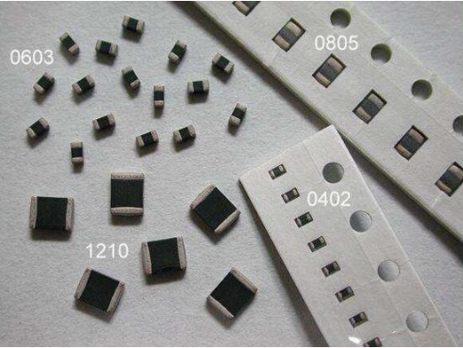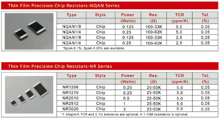
Thin and thick film resistors are the most common types in the market. They are characterized by a resistive layer on a ceramic base. Although their appearance might be very similar, their properties and manufacturing process are very different. The main difference is method the resistive film is applied onto the substrate.
The resistive layer of thin film is sputtered (vacuum deposition) onto a ceramic base. This creates a uniform metallic film of around 0.1 micrometer thick. Often an alloy of Nickel and Chromium is used (Nichrome). They are produced with different layer thicknesses to accommodate a range of resistance values. The layer is dense and uniform, which makes is suitable to trim the resistance value by a subtractive process.

With photo etching or by laser trimming patterns are created to increase the resistive path and to calibrate the resistance value. The base is often alumina ceramic, silicon or glass. Usually thin film is produced as a chip or smd resistor, but the film can also be applied onto a cylindrical base with axial leads. In this case, more often the term metal film resistor is used, such as Microhm Electronics HPMRY series.


